Industry News
10 Common Mistakes Beginners Make When Choosing Electronic Components (and How to Avoid Them)
When you’re just getting
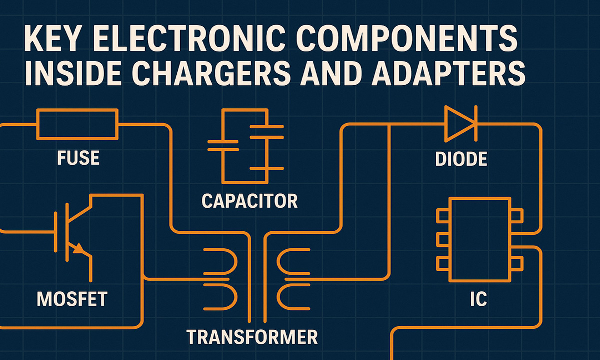
When a charger fails, overheats, or charges too slowly, the real problem is usually hidden on the PCB: the small resistors, capacitors, MOSFETs, transformers, and ICs that quietly manage power flow.
As a senior power-electronics engineer at a Tier-1 adapter manufacturer once put it: “From a reliability standpoint, the plastic case and logo don’t matter nearly as much as the capacitor bank, the main switch, and the isolation transformer. That’s where lifespan, safety, and efficiency are really decided.”
This article gives a practical, engineering-oriented look at the key electronic components inside modern chargers and adapters, how they work together, and which details matter most for reliability and performance.
Most phone and laptop chargers today are high-frequency switch-mode power supplies (SMPS). The basic power path looks like this:
AC input → EMI filter and protection → rectifier → high-frequency switch plus transformer → secondary rectifier and filter → feedback and control → output port (USB-A / USB-C / DC barrel)
On a high level:
• Input side: Handles surge, EMI, and rectification of AC mains (typically 100–240 V) into high-voltage DC.
• Primary side: A MOSFET (or GaN FET) chops the DC at high frequency (tens to hundreds of kHz), feeding the transformer.
• Transformer and isolation: Provides galvanic isolation between mains and low-voltage output, and steps voltage up or down as needed.
• Secondary side: Rectifies and smooths the low-voltage output for USB-A / USB-C ports.
• Control and feedback: Maintains constant voltage/current and negotiates fast-charging protocols (PD, QC, PPS, etc.).
Why component quality matters:
• Efficiency: Better MOSFETs, magnetics, and low-ESR capacitors mean lower losses and less heat.
• Safety: Fuses, MOVs, proper creepage/clearance, and insulation construction reduce shock and fire risk.
• Lifetime: Electrolytic capacitor quality and thermal design often decide whether a charger lasts 1 year or 5+ years.
Below is a concise overview of the most important components you’ll typically find inside a charger or power adapter.
Component overview table (text format):
| Component | Main function | Typical location | Key design considerations |
|---|---|---|---|
| Fuse / resettable fuse (PTC) | Over-current and short-circuit protection | AC input | Inrush capability, safety approvals, time-current curve |
| MOV (metal oxide varistor) | Surge and lightning protection | After fuse on AC input | Clamping voltage, energy rating, coordination with fuse |
| NTC thermistor (inrush limiter) | Limits inrush current at plug-in | Input or DC bus | Cold/hot resistance, power dissipation, thermal behavior |
| Common-mode / diff-mode chokes | EMI suppression | Input filter | Inductance, saturation current, leakage inductance, core material |
| Bridge rectifier | Converts AC to DC | After input filter | Forward drop, current rating, thermal design |
| Bulk capacitor (electrolytic) | Stores DC energy, smooths rectified voltage | High-voltage DC bus | Capacitance, voltage, ripple current, ESR, temperature and lifetime |
| Power MOSFET / GaN FET | High-frequency switching | Primary side | RDS(on), gate charge, breakdown voltage, thermal resistance |
| Main transformer | Isolation and voltage step-down | Between primary/secondary | Turns ratio, insulation system, leakage inductance, core loss |
| Secondary rectifier / FET | Rectifies high-frequency AC to DC | Secondary side | Voltage/current rating, forward drop, switching speed, efficiency |
| Output capacitors | Filter ripple, stabilize output | Near output connector | Capacitance, ESR, ripple rating, low-temperature behavior |
| Controller IC | PWM control and protections | Primary side | Supported topology, standby consumption, protections |
| Optocoupler + reference (e.g. TL431) | Feedback across isolation barrier | Between secondary/primary | CTR stability, linearity, isolation voltage |
| Current-sense resistor | Measures current for regulation/protection | Primary and/or secondary | Power rating, tolerance, temperature coefficient, PCB layout |
| USB-C PD / protocol IC | Negotiates PD, QC, PPS, etc. | Near USB-C port | Supported standards, firmware maturity, ESD robustness |
If your team needs a refresher on parameters like voltage rating, ESR, power dissipation, or tolerance, keep an internal “electronic components parameter guide” handy and use it when reading datasheets or negotiating with suppliers. For your site, this could be linked as: Electronic Components Parameter Guide
Field-failure analysis and RMA data in the charger and adapter industry tend to highlight a few recurring culprits:
• Electrolytic capacitors (dry-out, ESR increase, leakage)
• Power MOSFETs (over-voltage, over-current, or thermal stress)
• Transformers and inductors (insulation breakdown, poor winding quality)
• Secondary rectifiers (thermal runaway, overstress)
A reliability engineer at a global power-supply test lab summarized it this way: “If you control capacitor quality, transformer design, and MOSFET stress, you’ve already eliminated more than 70 percent of long-term field failures.”
3.1 Typical failure modes vs. user symptoms
| Component | Typical failure mode | What the user sees | Mitigation in design |
|---|---|---|---|
| Bulk/output electrolytics | Dry-out, ESR increase, leakage | Random shutdowns, noise, shorter lifetime | 105 °C long-life series, derating, good thermal path |
| Power MOSFET | Short/open due to overstress | Charger dead, fuse blown or breaker trips | Snubbers, proper derating, solid gate drive, clean layout |
| Transformer | Insulation breakdown, PD issues | Intermittent failure, safety risks | Certified insulation systems, surge tests, creepage/clearance control |
| Secondary rectifier | Thermal runaway, junction damage | Overheating, smell, very slow or no charging | Correct current/voltage rating, heatsinking, synchronous rectification where appropriate |
| USB-C PD controller | ESD damage, firmware bugs | Only 5 V output, no fast-charge negotiation | Strong ESD design, mature firmware, compliance testing |
3.2 Stress “chart” for key components (for easy conversion to a bar chart)
Relative stress level (1–5, higher = more stress):
Electrolytic capacitors ★★★★★ 5
Power MOSFETs ★★★★☆ 4
Main transformer ★★★★☆ 4
Secondary rectifiers★★★☆☆ 3
NTC / inrush limiter ★★☆☆☆ 2
USB-C PD / protocol IC ★★☆☆☆ 2
Resistors (sense, bleeder)★☆☆☆☆ 1
LED indicators ★☆☆☆☆ 1
For purchasing and design reviews, this simple ranking is a reminder to invest more effort in validation and supplier control for the first four categories.
4.1 Resistors
In chargers and adapters, resistors are not just generic parts:
• Current-sense resistors set over-current thresholds and current limits.
• Startup resistors feed initial current to the controller IC.
• Bleeder resistors safely discharge capacitors when the charger is unplugged.
• Voltage-divider resistors scale voltages for feedback and protection circuits.
Important parameters include power rating, tolerance (often 1 percent or better), temperature coefficient, pulse load capability, and mechanical strength after any lead forming.
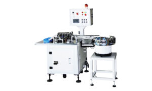
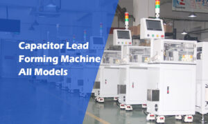
In high-volume production, consistent lead length and bending angles improve insertion efficiency and solder joint quality. Instead of manual bending, many factories use automatic resistor lead forming machines to keep dimensions accurate and reduce operator-induced stress. For example, you might promote a dedicated solution like: Resistor Lead Forming Machine
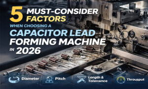
4.2 Capacitors
Chargers typically use a mix of:
• Aluminum electrolytic capacitors for bulk energy storage and smoothing.
• Ceramic capacitors (MLCCs) for high-frequency decoupling and EMI control.
• Polymer capacitors in higher-end designs for low ESR and improved lifetime.
Key design factors:
• Capacitance and voltage rating with appropriate derating
• ESR and ripple current rating
• Lifetime at elevated temperatures
• Behavior at low temperatures (especially for MLCCs)
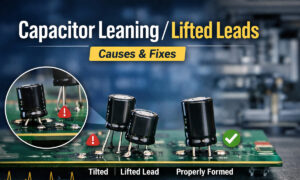
On the assembly line, poor lead forming or cutting can damage seals or cause micro-cracks that shorten capacitor life. Automated capacitor lead forming machines help minimize mechanical stress and maintain consistent lead geometry, which directly supports long-term reliability in compact charger PCBs. You can highlight a solution like: Capacitor Lead Forming Machine
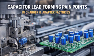
Even the best circuit design can fail prematurely if component handling and assembly processes are weak.
Common production-related issues include:
• Incorrect lead cutting and forming, which can stress component bodies or seals.
• Inconsistent lead length, affecting insertion depth and solder fillet quality.
• Manual bending that damages transformer insulation or cracks component cases.
• Poor control of soldering profiles, causing latent defects and early failures.
Best practices:
• Use automated forming equipment for resistors, capacitors, diodes, and other through-hole parts.
• Control insertion force and angle in wave-soldered designs.
• Keep clear work instructions linked to datasheet limits and derating rules.
• Implement incoming inspection plans focused on high-risk components such as electrolytic capacitors, MOSFETs, and transformers.
• Track field returns and tie them back to specific component lots and process changes.
Experienced manufacturing engineers often point out that what you save by skipping proper tooling and process control is quickly lost through rework, returns, and damage to your brand reputation.
Whether you are an OEM, a brand owner, or a procurement manager, you can evaluate charger and adapter suppliers with a structured checklist:
• Ask for a BOM summary focused on key components: capacitor brands and series, MOSFET part numbers, controller IC vendors, and transformer specifications.
• Check derating margins: operating voltage and current vs. component ratings, especially for capacitors, MOSFETs, and rectifiers.
• Review safety and compliance reports (CB scheme, UL/ETL, CE, etc.), and confirm that test conditions reflect real-world use.
• Request thermal test data at full load and elevated ambient temperatures (for example, 40–50 °C) to see how hot the hottest components get.
• Verify fast-charging protocols (USB-C PD, PPS, QC, etc.) with actual devices and programmable loads.
• Conduct or request tear-down inspections to verify component brands, creepage/clearance distances, isolation structures, and overall PCB quality.
• Pay attention to assembly details: uniform solder joints, clean separation between primary and secondary, and proper strain relief on input/output cables.
From an SEO and brand-building perspective, publishing transparent tear-down reports and explaining why you choose certain component brands or extra safety margins is a powerful way to demonstrate real-world expertise and trustworthiness.
Chargers and power adapters may look like simple “black boxes,” but inside they are carefully engineered systems built from fuses, MOVs, chokes, transformers, MOSFETs, capacitors, and sophisticated control ICs. The way you select, derate, and assemble these electronic components determines:
• Safety and compliance in global markets
• Energy efficiency and thermal performance
• Long-term reliability and RMA rates
• End-user experience and brand trust
By understanding which components are most critical, and by tightening both design rules and manufacturing processes, engineering and purchasing teams can:
• Ask better technical questions when qualifying charger suppliers
• Optimize their own charger platforms for efficiency, safety, and longevity
• Reduce warranty costs and protect their brand image in a competitive market
In short, strong component engineering plus disciplined production practices turn chargers and adapters from low-margin commodities into reliable, differentiated products that users trust and recommend.
When you’re just getting
Choosing the right capaci
A capacitor lead cutter i
Capacitor lead forming ma
Charger and power adapter
If your through-hole (rad