- Blog
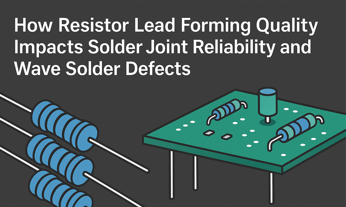
How Resistor Lead Forming Quality Impacts Solder Joint Reliability and Wave Solder Defect Rate
- By tian81259@gmail.com
Through-hole resistors still show up everywhere—power supplies, automotive ECUs, home appliances, industrial controls—because they’re cost-effective and mechanically robust. But in high-volume production, the “simple” resistor can become a hidden driver of rework if its leads aren’t formed consistently.
Resistor lead forming quality directly affects:
- Solder joint reliability (mechanical strength, thermal fatigue life, vibration tolerance)
- Wave solder defect rate (bridging, icicles, insufficient hole fill, opens, lifted leads)
- Process window (how forgiving your flux, preheat, and wave settings are)
If you want to reduce wave-solder defects without constantly tuning your solder pot, start upstream: lead forming.
Why Lead Forming Quality Matters More Than You Think
Wave soldering is a dynamic process. The solder wave interacts with lead geometry, pad design, hole size, flux activation, and thermal profiles—simultaneously. When resistor leads vary in length, bend angle, stand-off height, or insertion alignment, the wave no longer “sees” a repeatable joint.
That inconsistency shows up as:
- Uneven heating (some joints activate flux properly, others don’t)
- Variable wetting and capillary rise (hole fill becomes unpredictable)
- Changing solder drainage behavior (more bridging and icicles)
- Mechanical stress concentration (cracks after thermal cycling)
In short: poor forming creates assembly variation, and assembly variation becomes defects and reliability risk.
The 6 Lead-Forming Parameters That Drive Wave Solder Results
1) Lead Length Consistency (Protrusion Control)
After insertion, the lead protrusion on the solder side should be consistent. Too long and you get:
- Higher risk of bridging (extra metal in the wave path)
- More icicles and poor drainage
- Potential shorts in tight pitches
Too short and you risk:
- Insufficient fillet formation
- Lower mechanical robustness (less solder-to-lead bonding area)
Best practice: control cut length tightly and avoid burrs.
2) Bend Angle Accuracy (90° / 45° / Custom)
Bend angle affects:
- Insertion alignment
- Stand-off height
- Lead-to-hole contact consistency
Even small deviations can cause partial insertion or “spring-back,” which increases:
- opens (lead not properly seated)
- insufficient hole fill (gap breaks capillary action)
3) Stand-Off Height (Body-to-PCB Gap)
Stand-off height is critical for:
- Cleaning/flux behavior
- Heat flow into the joint
- Mechanical stress relief
If the resistor body is pressed too tightly to the board, you can see:
- flux entrapment / poor activation
- localized overheating of body coatings
- stress transfer into the solder joint during vibration
If stand-off is too high, you may get:
- weaker mechanical support
- lead wobble during wave contact → inconsistent fillets
4) Coplanarity and Lead Parallelism
For formed resistors (especially kinked or “dog-leg” styles), coplanarity affects whether both leads seat evenly. Poor coplanarity causes:
- one lead inserted deeper than the other
- uneven hole fill
- tilted components and “shadowing” effects in the wave
5) Lead Tip Quality (Burrs, Deformation, Oxidation Exposure)
Cutting and forming can damage plating or create burrs that:
- scrape hole walls during insertion (damaging PTH barrel)
- trap flux residues
- disrupt wetting and promote non-wetting / dewetting
A clean cut with controlled tip geometry improves repeatability.
6) Clinch / Retention Forming (If Used)
If you use clinch forming before wave solder:
- too aggressive clinch can lift pads or stress barrels
- too weak clinch can allow component float or movement in the wave
Retention must balance stability with board integrity.
How Poor Lead Forming Increases Wave Solder Defects
Bridging
Common forming-related contributors:
- excessive lead protrusion
- inconsistent lead spacing
- lead tilt changing the drainage path
Wave solder relies on proper solder drainage; geometry that “holds” solder increases bridges.
Icicles / Solder Spikes
Often tied to:
- long leads
- rough lead tips or burrs
- inconsistent exit angle that causes solder to “string” instead of detach cleanly
Insufficient Hole Fill / Opens
Strongly associated with:
- lead not centered in the hole (poor insertion due to forming error)
- gaps that reduce capillary rise
- leads that are too short or not fully seated
Lifted Leads / Skips (Non-wetting)
Can occur when forming introduces:
- plating damage
- contamination from handling or tooling
- mechanical stress that breaks flux film before proper wetting
How Forming Quality Impacts Long-Term Solder Joint Reliability
Even if a joint “passes visual,” forming quality can determine how it survives real life:
Thermal Cycling Fatigue
If the resistor is forced into position (misformed leads), the solder joint becomes a stress absorber. Repeated expansion/contraction can initiate:
- microcracks at the heel fillet
- barrel cracks in through-hole plating
- intermittent failures under temperature swings
Vibration and Mechanical Shock
Poor stand-off control and bent/loaded leads shift vibration energy into the solder joint rather than the lead. That increases:
- fillet cracking
- pad/barrel stress
- lead-to-solder interface separation over time
Field Serviceability
Consistent forming also improves:
- rework predictability
- replacement fit
- reduced pad damage during touch-up
A Practical “Control Plan” for Lead Forming + Wave Solder
If you want defect rate reduction you can measure, implement a simple control plan:
Incoming / Pre-process checks (Lead Forming)
- Cut length (target ± tolerance)
- Bend angle gauge check
- Stand-off height check
- Coplanarity check on a flat reference
- Tip burr inspection (visual/microscope sampling)
In-process checks (Insertion + Wave)
- Insertion seating verification (AOI or manual sampling)
- Lead protrusion sampling after insertion
- Wave solder defect Pareto by type (bridge, icicle, fill, skip)
Feedback loop
When wave defects spike, trace them back to the forming metrics first—before you change flux chemistry or wave speed.
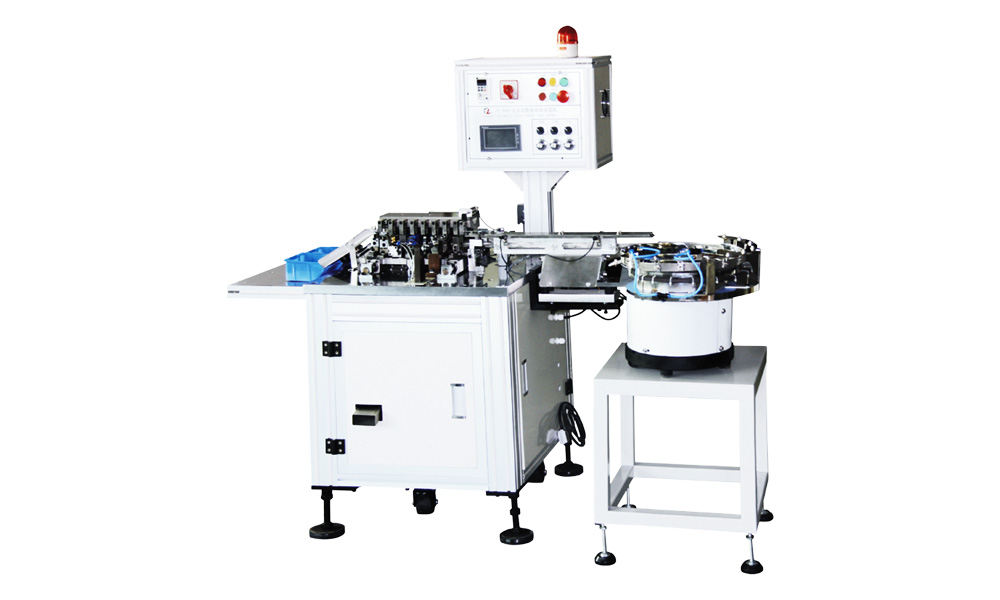
Why Automated Lead Forming Helps (Beyond Speed)
Manual or semi-manual forming often fails not because operators are careless—but because human variation is unavoidable at production scale.
A dedicated resistor lead forming machine improves wave outcomes by:
- delivering repeatable cut + bend geometry
- controlling stand-off and lead spacing
- reducing lead surface damage
- stabilizing insertion behavior (less tilt, less spring-back)
If you’re evaluating equipment, start here:
Quick Troubleshooting Map: Defect → Forming Cause
- Bridging high? Check lead protrusion length + lead spacing consistency
- Icicles high? Check cut quality (burrs) + protrusion length
- Hole fill low? Check insertion seating + bend angle accuracy + coplanarity
- Skips/non-wetting? Check lead surface damage/contamination from tooling
- Random opens? Check spring-back, lead alignment, and hole entry geometry
FAQ
What’s the fastest way to reduce wave solder defects related to resistors?
Standardize lead geometry first (length, angle, stand-off, coplanarity), then tune wave parameters. Stabilizing the inputs usually reduces defects faster than chasing solder pot settings.
Does better forming allow a wider wave solder process window?
Yes. Consistent geometry makes flux activation, heating, wetting, and drainage more repeatable—so the process tolerates normal drift in temperature, conveyor speed, and flux density.
Can lead forming quality affect PTH barrel reliability?
Yes. Misformed leads can scrape or stress the plated through-hole during insertion, increasing the risk of barrel cracks—especially after thermal cycling.
Takeaway
Wave solder defects and solder joint reliability aren’t only “wave solder problems.” They often start one step earlier—at lead forming. When resistors are formed consistently, you get a more stable wave process, fewer defects, and stronger joints that survive heat and vibration.
Share the Post:
Related Posts
20 Years of Expertise, Trusted by Clients Worldwide
The Preferred Choice of Foxconn, BYD, and Huawei