- Blog
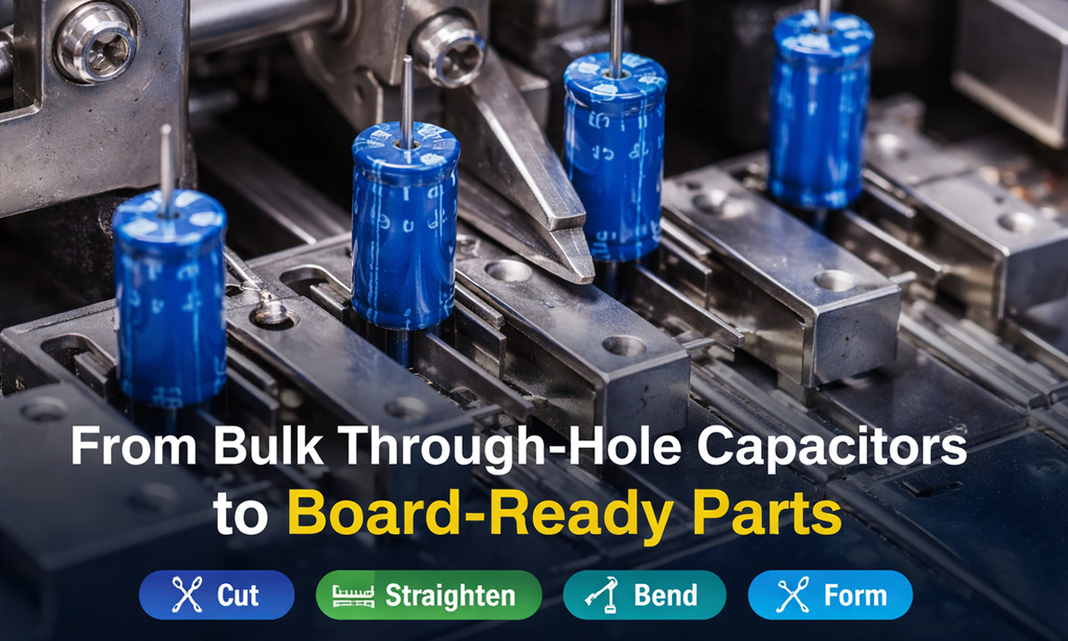
From Bulk Through-Hole Capacitors to Board-Ready Parts: The Complete Lead Prep Workflow
- By tian81259@gmail.com
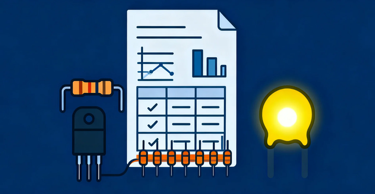
If you’ve ever tried to scale a through-hole (THT) capacitor line, you already know the truth: the capacitor itself isn’t the bottleneck—lead preparation is. Bulk capacitors arrive with long, easily deformed leads. Your PCB holes, assembly fixtures, and wave-solder process demand consistent lead length, pitch, and geometry.
This guide walks through the real factory workflow—from bulk capacitors → board insertion—covering lead cutting, lead straightening, lead bending, and lead forming, plus the most common defects and a practical QC checklist.
Why Lead Prep Matters More Than People Think
Even when the BOM and PCB are perfect, inconsistent lead prep causes:
- Mis-insertion and slow manual placement
- Bent leads that scrape plating or crack at the bend radius
- Poor wave-solder results (icicles, bridging, insufficient fillet)
- Rework loops that quietly destroy throughput
In high-mix production, lead prep is also where you win or lose on changeovers. The more repeatable your lead geometry is, the more stable your downstream processes become.
The Standard Workflow: Bulk → Board-Ready in 4 Stages
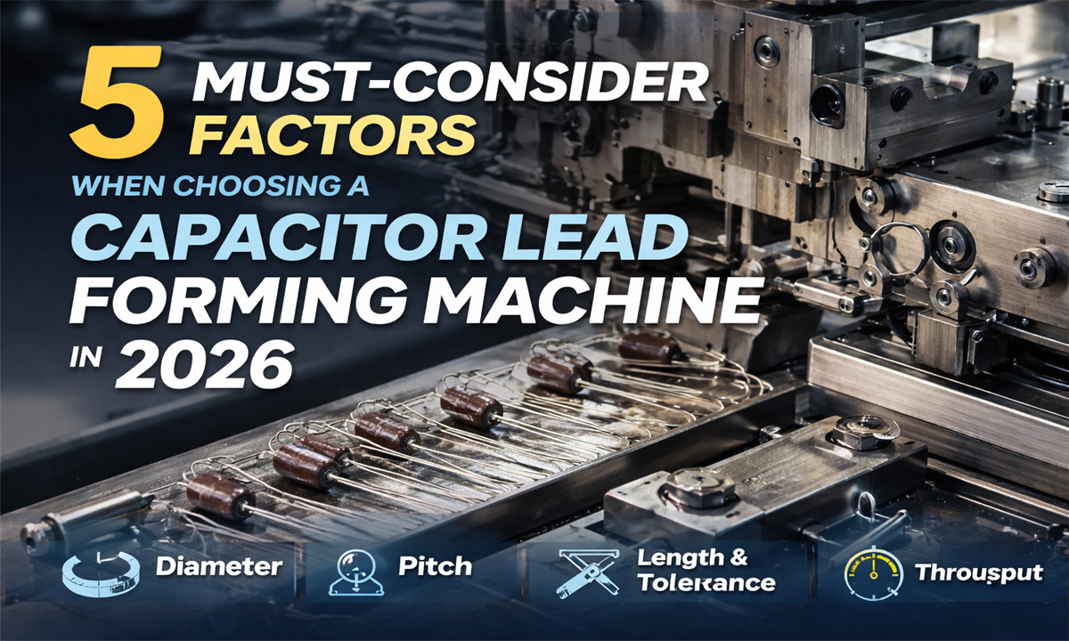
Stage 1 — Lead Cutting (Set the Length First)
Goal: Make every part the same “usable lead length” so insertion depth and solder wetting are consistent.
What happens here
- You define target lead length based on:
- PCB thickness
- Desired protrusion below the board (for wave solder fillet)
- Mechanical retention needs
- Component body clearance above PCB (for creepage/airflow)
Common cutting targets (general guidance)
- Many wave-solder lines aim for a controlled protrusion under the board rather than “as short as possible.”
- Too long → bridging and icicles
- Too short → weak fillet and pull strength risk
Typical defects to watch
- Burrs / sharp edges → flux trapping and solder spikes
- Lead deformation during cutting → insertion jams
- Length variation → uneven solder fillets across the board
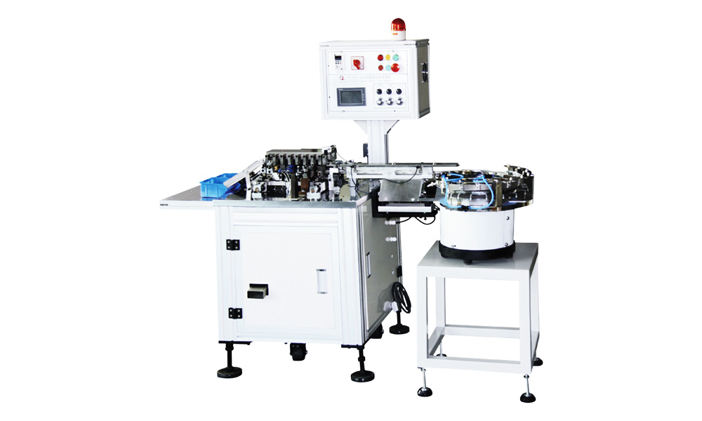
Internal link (example): If you want a dedicated cutting step with repeatable lead length control, see our capacitor lead cutting solution:Capacitor Lead Cutting Machine
Stage 2 — Lead Straightening (Restore Geometry Before You Bend)
Goal: Remove transport deformation so the next bending/forming step is accurate and doesn’t introduce stress cracks.
Bulk capacitors often arrive with:
- Slight lead “S” curves
- Leads splayed outward from packaging
- Micro-kinks near the seal (especially risky on electrolytics)
Why straightening is its own stage
If you bend a lead that’s already kinked, you’re effectively stacking stresses. That can lead to:
- Cracks in plating
- Reduced mechanical strength
- Inconsistent pitch after forming
QC check
- Leads should be straight enough to pass through a go/no-go gauge without forced alignment
- No visible kinks within the bend zone
Stage 3 — Lead Bending (Create the Basic Shape)
Goal: Establish the intended insertion style:
- Radial/vertical insertion
- Axial/horizontal mounting
- Special bends for clearance, height control, or vibration resistance
Key parameters
- Bend angle (commonly 90° for many styles)
- Bend radius (too tight increases crack risk)
- Bend position relative to capacitor body (avoid stressing seals)
Common defects
- Over-bending → wrong pitch, insertion force increases
- Under-bending → components sit crooked, height variation
- Bend too close to body → seal damage risk (electrolytics)
Best practice
Set a minimum safe distance from the body to the bend start, and keep it consistent with a fixed stop or tooling reference.
Stage 4 — Lead Forming (Lock in Pitch, Symmetry, and Repeatability)
Goal: Convert “rough bends” into a precise, repeatable geometry that matches PCB hole spacing (pitch) and insertion tooling requirements.
This is where you control:
- Final pitch (lead spacing)
- Lead parallelism
- Coplanarity and symmetry
- Final insertion-ready shape
Why forming is not the same as bending
Bending is the action. Forming is the precision outcome:
- Two bends that “look right” by eye can still have pitch errors that slow insertion and create solder defects.
Typical forming targets
- Pitch matched to PCB hole spacing with tight tolerance
- Lead legs parallel to reduce insertion force
- Consistent “stand-off” height so the capacitor body sits uniformly
Putting It Together: A Practical Line Setup (High-Mix Friendly)
Here’s a common, scalable sequence used in many PCB assembly environments:
- Incoming bulk capacitors (inspection + segregation by value/package)
- Lead cutting (length set)
- Lead straightening (remove deformation)
- Lead forming (pitch + final geometry)
- Tray/pack for kitting (keep formed leads protected)
- Insertion (manual or semi-auto)
- Wave solder (stable protrusion = stable fillet)
If you’re high-mix, the “hidden win” is building a repeatable parameter sheet per capacitor family (diameter, lead Ø, pitch, length target, bend distance, etc.).
Common Failure Points (and How to Fix Them)
1) Insertion Jams
Symptoms: Operators keep re-aligning leads by hand. Cycle time explodes.
Root causes
- Pitch variation from inconsistent forming
- Leads not parallel
- Cutting deformation near the lead tip
Fix - Add/upgrade forming control (stops, guides, consistent clamping)
- Ensure straightening occurs before forming, not after
2) Wave Solder Bridging / Icicles
Symptoms: solder spikes, bridges between leads, excess solder
Root causes
- Protrusion too long
- Burrs or rough cut surfaces
- Lead geometry inconsistent across the board
Fix - Re-define cutting length target to control protrusion
- Improve cut quality and verify burr control
3) Weak Fillets / Pull Strength Issues
Symptoms: thin fillets, incomplete wetting, poor mechanical retention
Root causes
- Leads too short under the board
- Inconsistent insertion depth due to lead length variation
Fix - Set a minimum protrusion standard and measure it
- Tighten lead length tolerance at the cutting stage
4) Lead Cracks Near the Bend
Symptoms: intermittent failures, visible micro-cracks, plating damage
Root causes
- Tight bend radius
- Bending after a pre-existing kink
- Bend too close to capacitor body
Fix - Straighten first
- Increase bend radius where possible
- Add a safe bend distance spec from the body
Quick Reference: What to Measure (QC Checklist)
Use this short checklist to keep your line stable:
- Lead length (post-cut): within tolerance
- Cut surface quality: no major burrs; no crushed tips
- Lead straightness: no kinks in bend zone
- Pitch (post-form): matches PCB hole pitch
- Parallelism: both leads insert smoothly without force
- Stand-off / seating height: consistent across samples
- Insertion force (spot check): should not require “wiggling”
Where Internal Linking Fits Naturally (SEO + UX)
If your site has related forming equipment or lead prep guides, the best internal links are placed where readers make decisions—right after you explain a pain point.
Internal link (example): For a broader look at lead prep consistency across multiple component types (useful if you also handle resistors/diodes), you can link to your forming lineup or process guide:Capacitor Lead Cutter Buying Guide
Final Thoughts
Bulk capacitors don’t become “board-ready” by accident. The difference between a smooth line and constant rework is almost always the same: repeatable lead geometry.
If you tighten up the sequence—cut → straighten → bend → form—and measure the right things (pitch, length, burrs, parallelism), you’ll see immediate improvements in:
- Insertion speed
- Wave-solder stability
- Rework rate
- Overall throughput
Share the Post:
Related Posts
20 Years of Expertise, Trusted by Clients Worldwide
The Preferred Choice of Foxconn, BYD, and Huawei