When you look at a PCB, the first thing that stands out is not the schematic – it’s the package types.
Whether a component is SMD or DIP directly affects PCB size, assembly method, automation equipment, repair strategy, and overall manufacturing cost. If you work in electronics design, purchasing, or production, understanding SMD vs DIP from a packaging perspective is foundational.
This article walks through the differences between SMD and DIP, how each fits into modern manufacturing, and how packaging choices connect to lead forming equipment and upstream/downstream processes in your factory.
1.What Are DIP and SMD, Exactly?
1.1 DIP (Dual In-line Package)
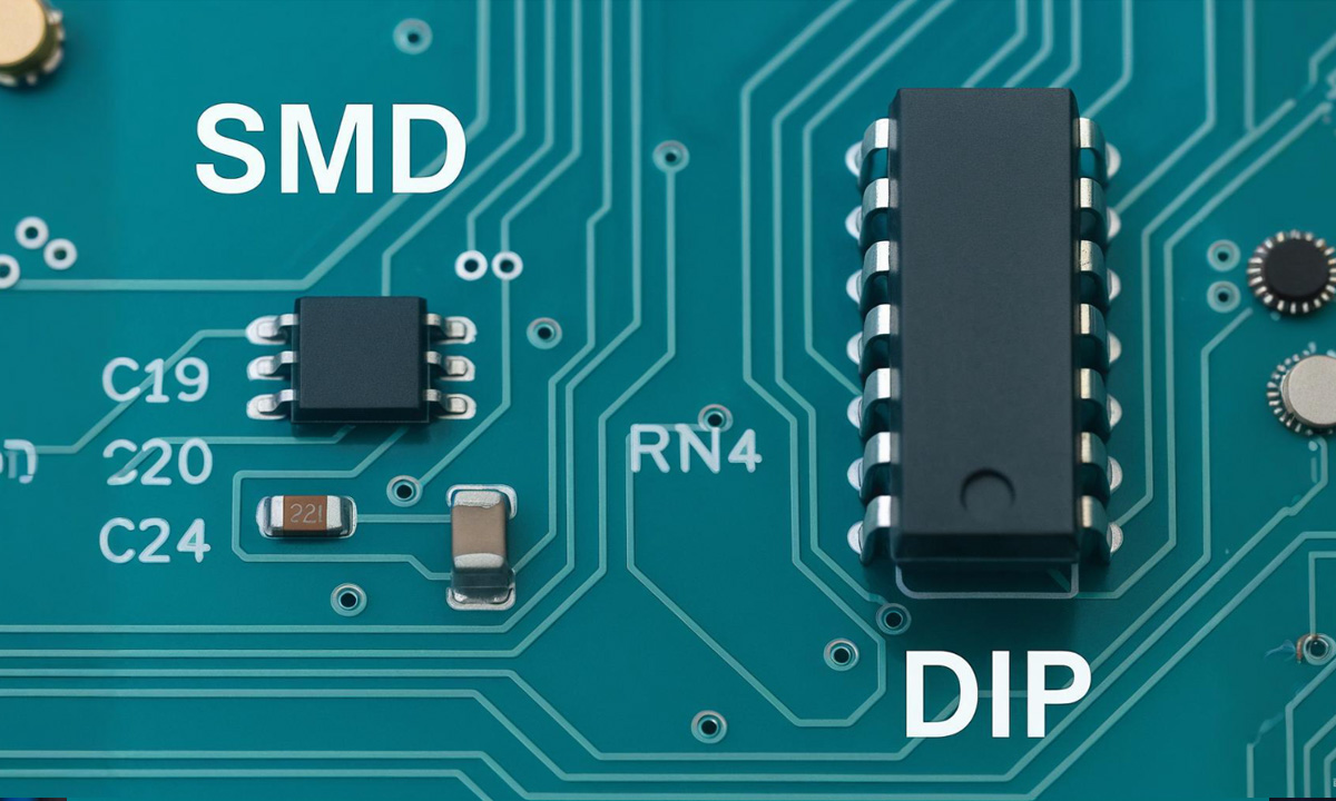
A Dual In-line Package (DIP) is a rectangular package with two parallel rows of pins protruding from the sides and bent downward so the leads pass through holes in the PCB. It is a classic through-hole package used for ICs, resistor networks, simple logic, memory, and many legacy devices.
Key characteristics:
- Mounting method: Pins go through drilled holes and are soldered on the opposite side of the PCB (manually or via wave soldering).
- Typical pin pitch: 2.54 mm (0.1″).
- Common pin counts: 8–40 pins for most commercial ICs.
- Typical use cases: Prototyping, socketed ICs, high-reliability or field-replaceable modules, industrial control, power supplies, educational boards.
Although many modern consumer products have moved to surface-mount packages, DIP is still widely used in power electronics, industrial equipment, and repair-friendly designs, where ease of replacement and mechanical robustness matter.
1.2 SMD (Surface Mount Device)
Surface Mount Devices (SMD) are components designed to sit directly on the surface of the PCB without going through drilled holes. They are assembled using Surface Mount Technology (SMT), where solder paste is printed on pads, components are placed, and then everything is reflow-soldered in a single pass.
Key characteristics:
- Mounting method: Leads or terminations land on flat pads on the same side of the PCB.
- Typical sizes: From relatively large SOIC packages down to tiny 0201 or 01005 chip resistors and capacitors.
- Typical use cases: Smartphones, wearables, chargers, adapters, LED drivers, power modules, and essentially all modern high-density electronics.
In short: DIP = through-hole, SMD = surface-mount. Once you see the package, you can immediately guess the assembly technology behind the product.
Package-Level Differences: Shape, Size, and Board Real Estate
2.1 Footprint and Board Density
- DIP takes more PCB area because of its wide body and two rows of relatively large-pitch pins. You also need drilled holes for every pin.
- SMD packages sit directly on the surface and can be much smaller for the same function. No holes are required (except vias), so routing density increases significantly.
For high-volume, space-constrained products like mobile chargers, adapters, or compact LED drivers, SMD packages are almost always preferred. DIP is more common in larger industrial power supplies, evaluation boards, or designs that prioritize robustness and reparability over size.
2.2 Mechanical Robustness and Handling
- DIP components are physically larger and easier to handle by hand. They are ideal for prototyping, test jigs, and low-volume production where technicians may insert components manually.
- SMD components are smaller and more fragile, requiring pick-and-place machines and proper reel/tape or tray packaging for automatic feeding.
From a packaging perspective, DIP is “human-friendly”; SMD is “machine-friendly”.
3.Assembly Process: Through-Hole vs Surface-Mount
3.1 DIP: Through-Hole Assembly Flow
A typical DIP-based assembly flow for resistors, capacitors, and ICs looks like this:
- Lead forming & cutting – component leads are cut to length and bent according to PCB hole spacing.
- Insertion – automatic insertion machines or operators place components into PCB holes.
- Wave soldering – boards pass over a solder wave; all through-hole joints are soldered simultaneously.
- Inspection & rework – joints are inspected and manually reworked if necessary.
For high-volume resistor or diode assemblies, manufacturers often integrate automatic lead forming before insertion to guarantee consistent lead pitch and height, which stabilizes both quality and insertion speed. If you’re handling large batches of axial resistors, a dedicated resistor lead forming machine can significantly reduce manual work and soldering defects in through-hole lines.
3.2 SMD: Surface-Mount Assembly Flow
An SMD-based line typically follows this sequence:
- Solder paste printing – solder paste is applied to pads using a stencil.
- Pick-and-place – SMD components are automatically placed onto paste-covered pads.
- Reflow soldering – the PCB passes through a controlled reflow oven to melt paste and form solder joints.
- Inspection (AOI / X-ray) – automatic optical inspection (AOI) and sometimes X-ray are used to verify solder quality.
SMD technology is optimized for high-speed, fully automated production. It eliminates the need for many drilled holes, shortens signal paths, and supports high-density designs that are not practical with DIP.
3.3 Mixed Technology Boards
Real-world PCBs often mix both technologies:
- SMD for small signal components and most ICs.
- DIP or other through-hole packages for large connectors, transformers, relays, and some power devices.
In mixed-technology designs, manufacturers frequently place SMD parts first (reflow), then insert DIPs and other through-hole parts and finish with wave soldering or selective soldering.
4.Electrical and Reliability Implications
4.1 Parasitics and High-Frequency Behavior
- DIP packages use longer leads, which introduce higher parasitic inductance and capacitance. At high frequencies, this can degrade signal integrity and increase EMI.
- SMD packages have shorter leads or leadless terminations, reducing parasitics and allowing better performance for high-speed digital and RF circuits.
For switching power supplies, high-frequency DC-DC converters, and RF modules, SMD packages are often chosen specifically for their better high-frequency behavior.
4.2 Thermal and Mechanical Considerations
- DIP components can be more tolerant of mechanical stress during handling and board flex, but may suffer under vibration if long leads resonate.
- SMD components, with their low profile and short terminations, generally show better vibration resistance when soldered properly.
For high-power devices (e.g., large MOSFETs, rectifiers, IGBTs), designers sometimes still prefer through-hole or bolt-down packages combined with dedicated heatsinks and insulating pads, especially in power electronics used in chargers, adapters, inverters, and industrial power supplies.
4.3 Serviceability and Field Repair
- DIP components are much easier to desolder and replace in the field, especially if sockets are used.
- SMD repair requires hot air tools, soldering skill, and often microscopes for fine-pitch packages.
For products meant to be serviced over many years, such as industrial control boards or certain power modules, designers may intentionally keep some critical ICs or passive networks in DIP or other through-hole packages.
5.Choosing SMD vs DIP for Your Design
There is no absolute “better” option – the right choice depends on product type, volume, cost structure, and repair strategy.
Aspect – DIP (Through-Hole) – SMD (Surface-Mount)
- PCB Size & Density – Larger footprint, lower density – Smaller footprint, high-density layouts
- Assembly – Manual or insertion + wave soldering – Fully automated SMT line + reflow
- Prototyping – Very convenient on breadboards – More difficult without adaptor boards
- High-Volume Cost – Higher labor and drilling cost – Lower cost per unit at scale
- High-Frequency Performance – Limited by parasitics of long leads – Better HF and EMI performance
- Field Repair – Easy to replace, especially in sockets – More difficult; requires special tools
- Typical Use – Industrial control, power, education – Consumer electronics, compact power supplies
As a rule of thumb:
- Use SMD for high-volume, compact products (chargers, adapters, LED drivers, consumer electronics).
- Use DIP or other through-hole packages where rugged connectors, high-power devices, or easy field replacement is essential.
6.Beyond SMD and DIP: Other Common Package Families
Once you understand the basic idea of “through-hole vs surface-mount,” other packages become easier to classify. Common IC and discrete packages include:
- SIP / SIL (Single In-line Package) – one row of pins; used for resistor networks and some power modules.
- SOIC, SOP – small-outline SMD versions of DIPs; shorter and narrower with bent-out gull-wing leads.
- QFP / LQFP – quad flat packages with leads on all four sides; common for MCUs and DSPs.
- BGA – ball grid arrays with solder balls on the bottom; ideal for high-pin-count processors and ASICs.
- Power packages such as TO-220, TO-247, D2PAK, etc. for MOSFETs, rectifiers, and regulators.
All of these fit into the same conceptual framework: how the package connects physically and electrically to the PCB.
7.Packaging, Procurement, and Production Equipment: Connecting the Dots
For purchasing managers and production engineers, understanding SMD vs DIP is not just a theoretical exercise. It directly impacts:
- Component selection and pricing – SMD reels vs bulk DIP components.
- Line configuration – SMT line, wave solder line, or mixed-technology.
- Required equipment – pick-and-place, reflow ovens, wave soldering machines, and lead forming equipment.
For buyers who need to define specifications, evaluate brands, and choose reliable distributors for resistors, capacitors, semiconductors, and other parts, our Electronic Components Procurement Guide provides a structured decision framework from requirement definition to supplier comparison.
On the production side, if your product family still includes a significant number of through-hole resistors or diodes, automating cutting and bending is one of the fastest ways to improve throughput and consistency on DIP-heavy lines. Our Lead Formers Buying Guide explains how to choose between different lead forming solutions and when it makes sense to invest in an automatic resistor lead forming machine for mass production.
8.FAQ: Common Questions About SMD vs DIP
8.1 Are SMD components always better than DIP?
Not always. SMD is better for miniaturization, high-volume production, and high-frequency performance. DIP is better for hand assembly, repairability, teaching, and some high-power or high-reliability applications where through-hole mounting is preferred.
8.2 Can I mix SMD and DIP on the same PCB?
Yes. Many industrial and power electronics boards use SMD for most passive components and small ICs and keep connectors, relays, transformers, or specific ICs in DIP/through-hole packages for mechanical strength or serviceability. The key is to design your process flow to handle both SMT reflow and through-hole soldering efficiently.
8.3 Does moving from DIP to SMD always reduce cost?
At high volume, SMD usually reduces cost due to higher automation, smaller PCB area, and fewer drilled holes. However, at very low volumes or during early prototyping, DIP may actually be cheaper and faster because you don’t need SMT stencils, reflow profiles, or specialized rework tools.
8.4 How does packaging affect reliability in harsh environments?
Both SMD and DIP can be reliable if designed correctly. SMD often provides better vibration performance due to shorter leads, while through-hole packages can offer stronger mechanical anchoring for large components like connectors or power devices. For harsh environments, factors like conformal coating, PCB material, and mechanical design of enclosures are just as important as the package itself.
8.5 Where do lead forming machines fit into all of this?
Lead forming machines are only relevant for through-hole components (DIP, axial resistors, radial capacitors, etc.). If your factory still processes significant volumes of such components, automating cutting and forming is one of the fastest ways to stabilize solder quality and reduce labor cost. In a fully SMT design, you won’t need lead forming – but in mixed or legacy products, it remains a critical link between component packaging and final PCB quality.
Conclusion
Understanding the difference between SMD and DIP from a packaging perspective helps you read a PCB at a glance, communicate better with suppliers, and choose the right manufacturing equipment for your product roadmap – whether you’re building compact phone chargers, robust industrial power supplies, or anything in between.
For teams that still rely heavily on through-hole components, it’s important to look not only at which packages you choose, but also at how you automate the related processes – from lead forming to final soldering – to improve quality, consistency, and overall production efficiency across your entire product line.