From smartphones under 6 mm thick to ultra-light laptops and wearables, “thin and light” has gone from a selling point to a default expectation. Most mainstream phones today sit around 8–9 mm, while 2025’s ultra-thin flagships have pushed thickness down into the 3.6–5.9 mm range. WIRED That design direction doesn’t just affect enclosures and batteries—it rewrites the rules for electronic components themselves.
To keep up, resistors, capacitors, ICs, and power devices must deliver higher performance in smaller footprints while integrating more functions onto fewer packages and layers. That raises the bar for design, manufacturing, and even automation equipment on the factory floor.
Thin Devices Start With Tiny, Highly Integrated Components
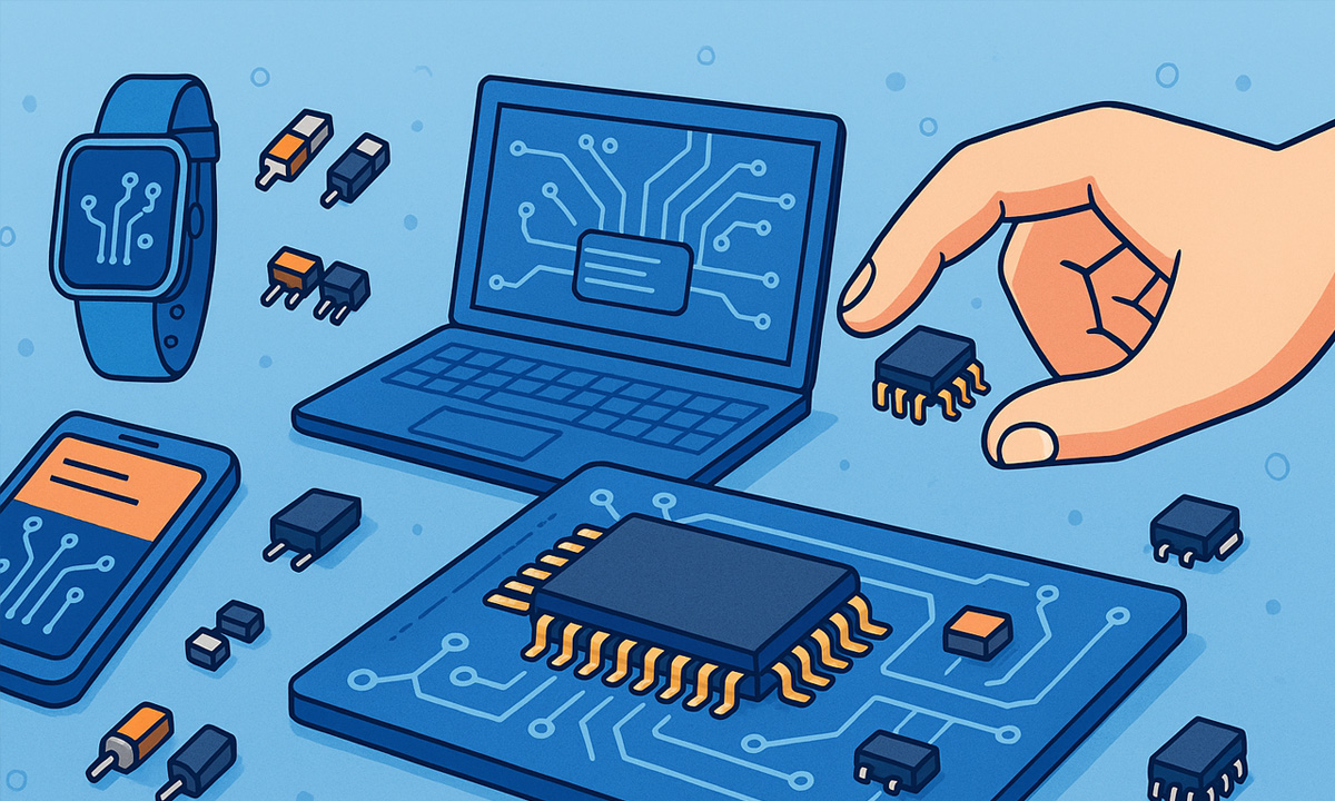
In the electronics industry, miniaturization means shrinking components and assemblies without sacrificing performance or reliability. It’s a core driver behind modern consumer devices—from smartphones and tablets to smartwatches and earbuds. Circuits-Central+1
Several trends converge here:
- Users want slimmer devices with bigger batteries and more features.
- Brands want to differentiate through design, not just performance.
- Engineers must fit radio, power, sensing, and processing into ever-smaller volumes.
To achieve that, designers rely heavily on:
- High-density interconnect (HDI) PCBs with microvias and fine line/space.
- System-in-package (SiP) and SoC that combine multiple functions into one package.
- Ultra-small surface-mount passives like 0402, 0201, and even 01005 series.
The HDI PCB market alone reached about USD 9.1 billion in 2024 and is projected to climb to USD 13.9 billion by 2033, driven largely by compact, high-performance consumer electronics. IMARC Group That’s a direct reflection of how important dense layouts and highly integrated components have become.
How Small Are Modern SMD Components, Really?
For anyone working in consumer electronics, SMD package codes like 0603 or 0201 are now everyday vocabulary. But it’s worth stepping back to see how dramatic the size reduction really is.
Common SMD resistor/capacitor package sizes include: Sierra Circuits+1
| Package | Approx. Size (mm) | Typical Use in Consumer Electronics |
|---|---|---|
| 1206 | 3.2 × 1.6 | Older designs, higher power passives |
| 0603 | 1.6 × 0.8 | General-purpose passives, many phones and tablets |
| 0402 | 1.0 × 0.5 | High-density smartphones, wearables, IoT nodes |
| 0201 | 0.6 × 0.3 | RF modules, space-constrained boards |
| 01005 | 0.4 × 0.2 | Extreme miniaturization, select mobile/medical designs |
At the 01005 level, the component’s length is only about four times the diameter of a human hair. At that scale:
- Parasitic effects (ESL, ESR, stray capacitance) become significant.
- Assembly precision and solder paste volume control are critical.
- Inspection often requires advanced optical or X-ray systems.
In parallel, miniaturization at the PCB and packaging level has driven component packages to sizes comparable to early IC design rules, forcing new approaches in package design and assembly. assets.new.siemens.com
Key Technical Requirements for Miniaturized, Highly Integrated Components
1. Electrical Performance and Signal Integrity
In thin, highly integrated devices, signal paths are short, dense, and often running at high frequencies:
- High-speed interfaces (USB-C, PCIe, LPDDR, MIPI) tolerate much less parasitic inductance and capacitance.
- RF front-ends in smartphones and wearables require tight control of matching networks built from very small passives.
- Power management ICs must switch at higher frequencies to use smaller magnetics and capacitors, increasing EMI and layout sensitivity.
Miniaturized components are selected not only on value and tolerance, but also on:
- Package parasitics and ESR/ESL.
- Temperature stability across a wide operating range.
- Compatibility with HDI stackups and controlled-impedance routing.
2. Thermal Management and Power Density
Thinner devices don’t leave much room for heat spreaders and large heatsinks. At the same time:
- SoCs and power stages can pack multiple watts of dissipation into a small footprint.
- Batteries are squeezed to maintain capacity while giving up physical volume.
- Aluminum or magnesium alloy housings double as thermal paths.
This forces component-level requirements such as:
- Low-loss materials for inductors and capacitors to reduce self-heating.
- Package designs optimized for thermal conduction to the PCB or chassis.
- Tighter derating rules for power components, especially in adaptive fast-charging designs and high-current DC-DC converters.
3. Mechanical Reliability Under Flex, Drop, and Vibration
Thin devices are more prone to bending and impact. That means:
- Small SMDs near board edges experience higher mechanical strain, increasing the risk of cracked solder joints or component fractures.
- Connectors, switches, and larger components must withstand torsion and local flex without transferring stress to tiny passives and ICs.
As a result, engineers evaluate:
- Board stackup and thickness to balance stiffness vs. flex.
- Component placement rules (keep-outs around mounting holes, slots, or scoring lines).
- Reinforcement strategies such as underfill, corner bonding, or localized stiffeners.
4. Manufacturability, Yield, and Automation
As components shrink, the process window narrows:
- Stencil design and solder paste volume must be tightly controlled to avoid tombstoning or bridging on 0201/01005 packages.
- Pick-and-place machines need high accuracy and repeatability at very high throughput.
- For through-hole parts that remain (e.g., high-voltage film capacitors, large resistors, power devices), lead forming consistency becomes more critical so they fit dense PCBs without stressing pads or traces.
This is where automation equipment directly influences whether a design can be built at scale.
For example, through-hole resistors that sit close to tightly packed ICs still need precise lead length and standoff to keep solder joints reliable. An automatic
resistor lead forming machine helps ensure every lead is cut and bent to the same dimensions, reducing manual bending, PCB stress, and variability in solder fillets.
Integration at the Package and Board Level
System-in-Package (SiP) and Multi-Chip Modules
To support thin form factors while adding more functions (5G, Wi-Fi 7, GNSS, secure elements, sensors), many designs move to:
- SiP modules combining RF front-ends, filters, passives, and sometimes controllers in a single package.
- Multi-chip power modules that combine drivers, MOSFETs/IGBTs, and protection circuits.
These integrated modules:
- Reduce routing complexity on the PCB.
- Improve electrical performance by shortening internal interconnects.
- Allow the main board to be smaller and simpler, especially in wearables and TWS earbuds.
But they also demand:
- Advanced substrate technologies (organic interposers, embedded passives).
- More sophisticated thermal and reliability validation at module level.
HDI PCBs and Microvias
As noted above, the HDI PCB market is growing steadily because consumer devices need more interconnect density in less area. 战略市场研究+1
HDI techniques—microvias, blind/buried vias, and fine line/space rules—enable:
- Higher I/O density around BGAs and fine-pitch QFNs.
- Shorter signal paths and better signal integrity in high-speed designs.
- Room for larger batteries or mechanical components inside thin housings by shrinking PCB footprint.
However, HDI requires very controlled fabrication and assembly processes, and any inconsistency in component dimensions or lead forming can quickly hurt yield.
What This Means for Component Selection and Supply Chain
For OEMs, ODMs, and EMS providers in the consumer electronics space, thin-and-light design trends translate into concrete checklists:
- Component Libraries Must Be Miniaturization-Ready
- Prefer 0402 and 0201 passives as default where process capability allows.
- Maintain a clear derating policy and application notes for when to go down to 01005.
- Datasheets Need More Than Just “Value + Voltage”
Purchasing and engineering teams must look at:- Package parasitics and high-frequency behavior.Thermal resistance and power ratings in compact footprints.Mechanical robustness and solder joint reliability data.
electronic component parameter guide can help your team standardize how they choose parts for high-density, thin devices. - Assembly and Pre-Forming Processes Must Match PCB Density
- Even in highly miniaturized designs, many consumer products—especially power supplies, chargers, and adapters—still rely on:
- Large electrolytic capacitors for bulk energy storage.Film capacitors and power resistors in high-voltage or high-current paths.
capacitor lead cutting and forming machine can pre-bend and trim leads so large capacitors sit cleanly on the board, respect creepage/clearance, and avoid mechanical interference with low-profile housings and neighboring SMDs.
Preparing Your Factory for the Next Wave of “Thin and Light”
As consumer electronics continue to slim down while packing in more features, the demands placed on components and production lines will only increase. Practical steps for staying ahead include:
- Audit your BOMs for oversized packages and legacy components that block miniaturization.
- Upgrade your design rules to include HDI capabilities and finer SMD footprints where your EMS partners can support them.
- Align mechanical and electrical teams so housing, battery, PCB, and component choices are co-designed, not handled in isolation.
- Invest in precision automation, from high-speed pick-and-place equipment to reliable component forming machines, to keep yield and consistency under control even as components shrink.
- Leverage real data—from field failures, reliability tests, and supplier process capabilities—to refine your component approval lists.
Thin, lightweight devices are no longer a niche—they’re the baseline. The brands and factories that can pair aggressive industrial design with robust miniaturized, highly integrated electronic components will be the ones that stay competitive in the next generation of consumer electronics.
Q1: What is miniaturization of electronic components in consumer electronics?
A1: Miniaturization of electronic components refers to shrinking resistors, capacitors, ICs, and power devices to smaller packages such as 0402, 0201, or even 01005, while maintaining electrical performance, thermal reliability, and mechanical robustness in thin and light devices.
Q2: Why do thin consumer electronics require highly integrated components?
A2: Thin smartphones, tablets, and wearables have limited internal space but higher performance demands. Highly integrated components such as SoC, SiP modules, and HDI PCBs combine multiple functions into fewer packages, freeing room for larger batteries and advanced features without increasing device thickness.
Q3: How do precision lead forming machines support miniaturized designs?
A3: Even in high-density designs, through-hole resistors and capacitors are still widely used in power and high-voltage sections. Precision resistor and capacitor lead forming machines cut and bend leads consistently, ensuring accurate fit, stable solder joints, and high yield on crowded PCBs used in thin consumer electronics.