
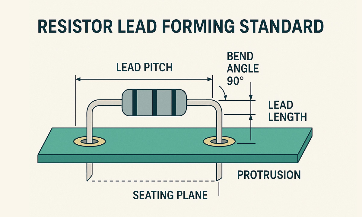
When your resistors appear on multiple PCB layouts (different hole patterns, board thicknesses, soldering methods, and clearance constraints), “just match the footprint” isn’t enough. What you actually need is a single, documented forming standard—one that converts PCB variation into a small set of controlled parameters your forming process can reproduce every time.
Below is a practical way to define a unified standard for resistor forming angle, lead length, and bend geometry—grounded in widely used electronics workmanship and design guidance.
Why a unified forming standard matters
A consistent lead-form spec improves:
- Solder quality and inspection pass rate (less underfill, fewer cold joints, fewer “lead too long/too short” defects)
- Electrical spacing safety (reduced short risk from excessive protrusion)
- Manufacturing efficiency (fewer “special cases,” fewer setup changes, easier QA gauging)
- Reliability (less lead stress, less spring-back, better mechanical restraint)
High-reliability workmanship standards emphasize that reliable soldered connections come from a combination of proper design, process control, trained personnel, and careful workmanship.
Step 1: Classify PCB layouts into “forming families”
Instead of creating a new forming spec for every PCB, group layouts into forming families using a few variables that actually change the lead requirements:
- Supported vs. unsupported holes
Workmanship criteria differ depending on whether the plated-through hole is supported by pads/lands on both sides and how the joint is formed. (This is reflected in common acceptance tables for through-hole connections.) - Board thickness (T)
Thicker boards can “eat up” lead length and change what’s visible at the solder side, especially when component leads are pre-trimmed. - Soldering process (wave / selective / hand / intrusive)
Process affects how much protrusion is safe and how fillets form. Many standards describe a goal of full hole fill with good wetting to lands, lead, and barrel. - Clearance constraints (creepage/clearance, nearby pins, enclosure height limits)
This drives your maximum lead protrusion limit.
Result: most factories end up with 2–4 families (e.g., “Class 2 supported holes on 1.6mm boards,” “Class 3 supported holes,” “unsupported holes requiring clinch,” etc.), not 40 different special specs.
Step 2: Set a single “lead protrusion window” (the output you must hit)
Your “unified” spec should start with what matters at the solder joint: how much lead is allowed to stick out after soldering.
A widely used acceptance reference provides clear protrusion guidance for supported holes, including:
- Minimum: the end is discernible in solder (Class 2 / Class 3)
- Maximum: 2.5 mm for Class 2; 1.5 mm for Class 3 (supported holes)
It also notes protrusion should not exceed 2.5 mm if it could violate electrical spacing or create handling risks.
Practical unified rule (common in production)
Pick one protrusion window per quality target:
- If you build to “high reliability / Class 3 style”: target 0.8–1.5 mm
- If you build to “general electronics / Class 2 style”: target 0.8–2.5 mm (but only if spacing allows)
That single window becomes the anchor for every layout.
Step 3: Convert PCB variation into one lead-length formula
Once protrusion is defined, you can standardize lead length with a simple stack-up:
Final formed lead length (from seating plane to lead tip)
L = T + P + A
Where:
- T = PCB thickness
- P = required protrusion (your chosen window)
- A = allowance for clinch/retention bend (if used) or for post-solder trim strategy
If you’re not clinching and you pre-trim before insertion, A can be 0–small.
If you are clinching, A includes the clinch geometry so you don’t “steal” length from protrusion.
Also document how you measure. One widely used soldering standard explicitly notes measurement is made from the “end of the part,” including coatings/seals/beads where applicable—small detail, big difference when suppliers vary.
Step 4: Standardize bend geometry (this protects the component and improves repeatability)
Across different PCB layouts, the most common failure mode in “unified specs” is ignoring bend radius and straight length before the bend—which causes cracked seals, weakened leads, spring-back, and inconsistent pitch.
A common workmanship reference for lead forming includes:
- Leads should extend at least one lead diameter (or thickness), but not less than 0.8 mm, before the bend radius begins
- Minimum bend radius depends on lead diameter (e.g., 1× to 2× lead diameter/thickness depending on size range)
Practical unified bend spec (easy to enforce)
Define these as global rules:
- Straight-before-bend (SB): ≥ max(0.8 mm, 1× lead diameter)
- Bend radius (R):
- lead < 0.8 mm → R ≥ 1× diameter
- 0.8–1.2 mm → R ≥ 1.5× diameter
- 1.2 mm → R ≥ 2× diameter
These two numbers dramatically reduce “same setting, different result” across resistor vendors.
Step 5: Define “forming angles” as a controlled output—not a guess
For axial resistors, you typically only need a few standardized forms:
A) Horizontal mount (most common)
- Bend angle: 90° (both leads)
- Lead pitch (hole-to-hole): matches PCB footprint family (e.g., 7.5 mm / 10 mm / 12.5 mm)
- Tolerances (example you can adopt):
- Angle: 90° ± 3°
- Pitch: ± 0.2 mm (or tighter if your insertion machine requires it)
- Lead length (L): ± 0.3 mm (choose based on your process capability)
B) Vertical mount (space-saving)
- One lead acts as the “post,” the other wraps/returns depending on the footprint.
- Vertical mounting often needs additional attention to clearance and mechanical support expectations in workmanship guidance.
Key point: you don’t need 20 angles. You need 2–3 standardized forms plus family-specific pitch/length targets.
Step 6: Add one solder-joint reality check (so your forming spec doesn’t fight soldering)
Your forming standard must avoid placing the bend where solder fillet formation needs to occur. Industry guidance commonly notes the solder fillet should extend up the lead a minimum of one lead diameter or 2.5 mm (whichever is less), and if bends are present the fillet should not extend past the bend. resources.pcb.cadence.com
So, in your unified spec:
- Ensure the bend location is above the expected fillet zone
- Or you’ll see chronic “insufficient wetting” / “fillet stops at bend” issues even when operators do everything right
Step 7: Document the standard as a “Forming Control Sheet” (what QA and production actually use)
Include these fields (keep it to one page):
- Quality target (e.g., “Class 2 style” vs “Class 3 style”)
- PCB family definition (supported/unsupported holes, thickness range)
- Form type (Horizontal / Vertical)
- Pitch (P)
- Protrusion window (min/max)
- Lead length formula and target (L)
- Bend rules (SB, R)
- Measurement method + gauge method
- Sampling plan (first article + hourly checks)
Implementation tip: use recipe-based forming to reduce changeovers
If you’re running mixed PCB layouts, a recipe approach (pitch + L + form type) is the fastest way to keep “unified standards” real on the shop floor.
If you’re building/expanding forming capacity, these pages are directly relevant for your internal linking:
- FL-612 High-Precision Resistor Horizontal and Vertical Integrated Forming Machine (recipe-friendly because it supports both orientations by changing molds)
- Essential Equipment List for Resistor Lead Cutting and Forming