
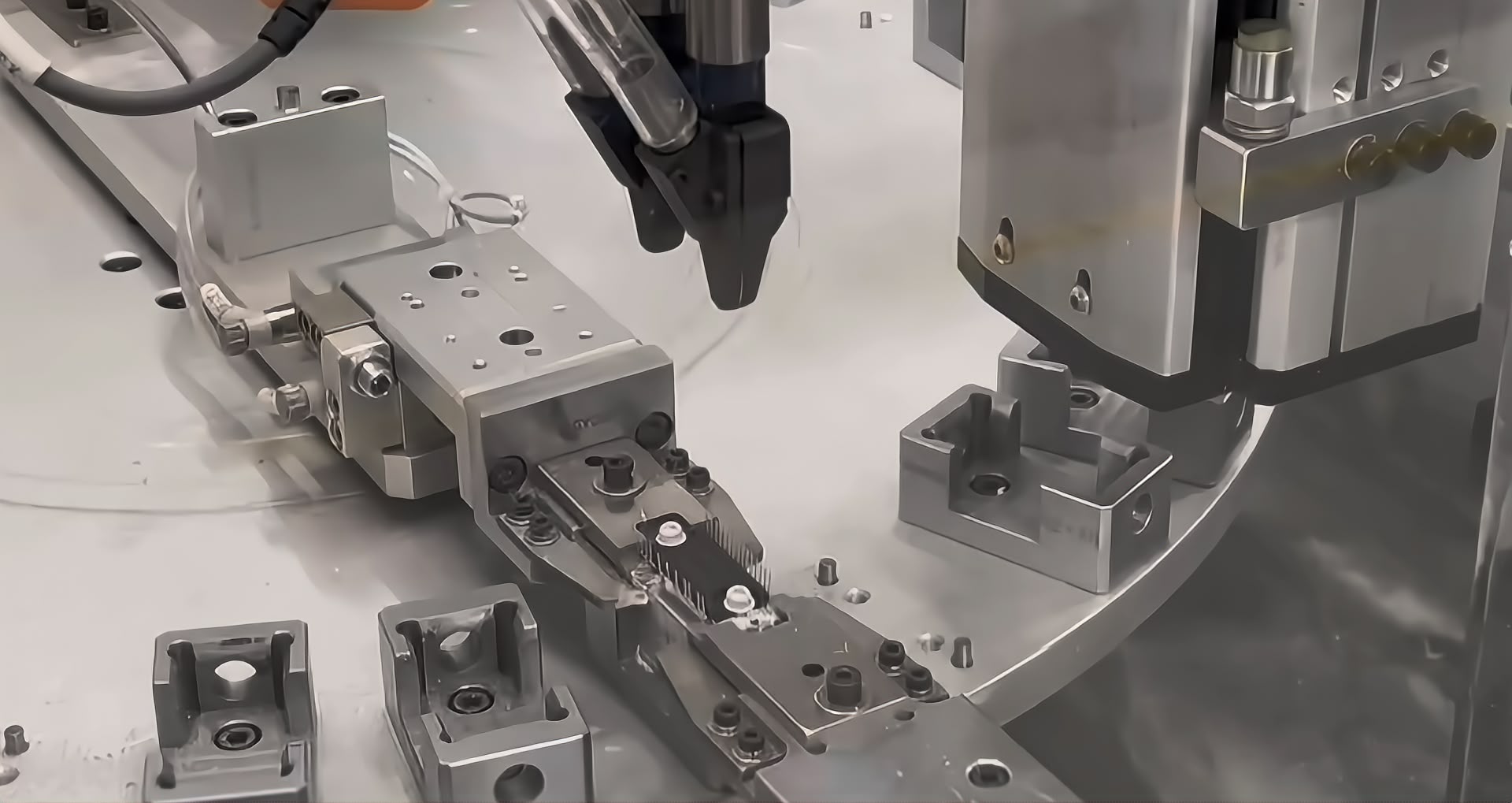
Transistor lead forming shapes should be selected according to the final mounting position, PCB hole pattern, required clearance, heatsink location, and assembly sequence. These profiles can be produced using manual tooling, pneumatic equipment, or dedicated transistor lead forming equipment, depending on the component package, production volume, and required repeatability.
For direct PCB insertion, straight-cut or slightly spread leads are usually sufficient. When a transistor must lie parallel to the PCB or connect to a nearby heatsink, 90-degree, offset, or compound bends may be required. The forming dimensions should always be defined from a fixed package datum and verified with the actual transistor, PCB, heatsink, and insulation materials.
A suitable forming process must achieve the required dimensions without cracking the plating, twisting the leads, stressing the lead-to-body interface, or causing poor PCB insertion.
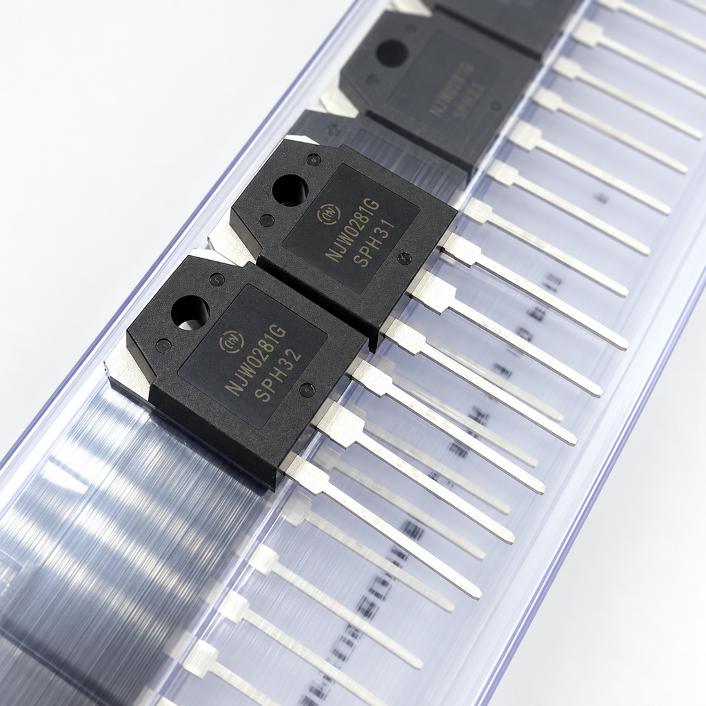
Why Transistor Leads Require Forming
Power transistors, voltage regulators, MOSFETs, IGBTs, bridge rectifiers, and other through-hole semiconductor packages are normally supplied with straight leads. However, their incoming configuration may not match the final assembly.
Lead forming may be required to:
- Match the PCB hole pitch
- Change the mounting direction
- Align the package with a heatsink
- Maintain electrical clearance
- Establish a controlled standoff height
- Prevent the package body from contacting the PCB
- Compensate for differences between the package and PCB layout
- Prepare components for automated insertion or assembly
- Reduce manual adjustment during final installation
Packages that commonly require customized lead forming include:
- TO-92
- TO-126
- TO-220
- TO-247
- TO-3P
- IGBT packages
- Voltage-regulator packages
- Power-diode packages
- Bridge rectifier packages
When the incoming package, PCB layout, or finished profile falls outside a standard configuration, the process should be evaluated as a custom component forming application.
A package name alone is not enough to define the forming process. Official package drawings show dimensional ranges rather than one fixed value, and packages with the same general designation may still differ between manufacturers. For example, TO-220 and TO-247 drawings specify body, lead, pitch and mounting-hole dimensions using minimum and maximum values. ti.com
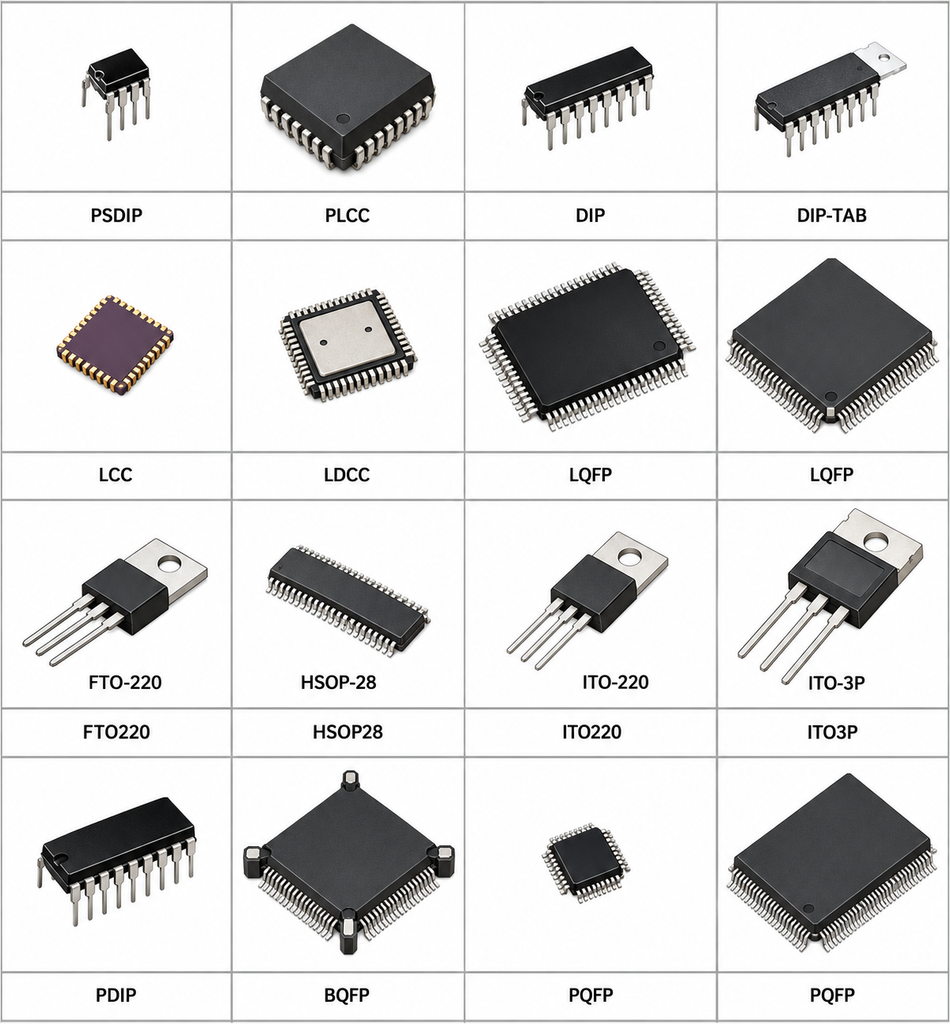
Common Transistor Lead Forming Shapes
| Forming shape | Typical application | Main dimensions to control | Main production risk |
|---|---|---|---|
| Straight cut | Vertical PCB mounting | Lead length and cut consistency | Burrs and unequal lengths |
| Lead spreading | PCB pitch adjustment | Final pitch and symmetry | Twisted or nonparallel leads |
| 90-degree bend | Horizontal PCB or heatsink mounting | Bend position, angle and height | Package stress and poor coplanarity |
| Offset or Z-bend | Position correction and clearance | Offset, height and two bend positions | Accumulated dimensional error |
| Standoff forming | Controlled distance above PCB | Standoff height and coplanarity | Unstable seating |
| Inward forming | Narrower PCB hole pattern | Reduced pitch and centering | Lead interference |
| Outward forming | Wider PCB hole pattern | Expanded pitch and symmetry | Excessive outer-lead stress |
| Compound forming | PCB and heatsink alignment | Multiple heights, angles and offsets | Difficult tooling and changeover |
PCB Mounting Configurations
Vertical PCB Mounting
In vertical mounting, the package body is approximately perpendicular to the PCB.
Common forming options include:
- Straight cut
- Lead spreading
- Inward forming
- Small standoff features
Vertical mounting is generally compact in PCB area but increases the assembled height.
Important checks include:
- Component height
- PCB hole pitch
- Lead insertion length
- Package clearance
- Stability before soldering
- Distance from neighboring components
Horizontal PCB Mounting
In horizontal mounting, the package body is approximately parallel to the PCB.
Common forming options include:
- 90-degree bending
- Offset bending
- Standoff forming
- Compound bending
Horizontal mounting reduces assembly height but may occupy more PCB area.
The design must control the distance between the package and PCB. Direct, uncontrolled contact may interfere with cleaning, insulation, heat transfer, or mechanical stability.
PCB Mounting With an Attached Heatsink
A small heatsink may be attached to the transistor before or after PCB insertion.
The forming profile must account for:
- Heatsink weight
- Mounting-hole position
- Insulating pad thickness
- Thermal interface material
- Screw position
- PCB hole location
- Assembly sequence
- Mechanical load on the solder joints
The transistor leads should not be used to force a misaligned heatsink into position.
Lead Forming for Heatsink Assembly
For a heatsink-mounted transistor, the package body, mounting hole, PCB and heatsink must align simultaneously.
A typical assembly may contain:
- Transistor
- Heatsink
- Insulating pad
- Insulating bushing
- Thermal grease
- Screw and washer
- PCB
- Formed leads
TO-247 packages, for example, are commonly defined as heatsink-mounted through-hole packages, but the exact body, lead and mounting-hole dimensions still depend on the selected package outline. Nexperia
For stable, high-volume production, an automatic transistor lead forming machine can combine component feeding, positioning, cutting, and forming within one production cycle.
Forming Before Heatsink Assembly
This sequence is suitable when:
- The forming machine locates the transistor body directly
- The formed component can be inspected independently
- The heatsink assembly process is separate
- The package position remains stable during screw fastening
Advantages:
- Easier dimensional inspection
- Simpler forming fixtures
- Clear separation between forming and assembly defects
Potential problem:
- The finished leads may be deformed during later heatsink installation.
Forming After Heatsink Assembly
This sequence may be used when:
- The heatsink becomes the assembly datum
- The transistor position depends on the insulating pad and screw
- Several transistors share one heatsink
- Final lead positions must match the PCB after mechanical assembly
Advantages:
- Lead position can be related to the assembled heatsink
- Useful for complex multi-transistor assemblies
Potential problems:
- The fixture becomes more complicated
- The tool must avoid damaging the heatsink
- Variation in screw fastening or pad thickness can affect the lead position
Integrated Forming and Heatsink Assembly
For stable, high-volume products, forming may be integrated with:
- Thermal grease application
- Insulating-pad placement
- Transistor positioning
- Heatsink loading
- Screw fastening
- Presence inspection
- Torque monitoring
- Finished assembly discharge
Integration can reduce manual handling, but it requires stable component and assembly specifications.
Dimensions That Must Be Defined
A reliable finished-component drawing should include the following dimensions.
| Dimension | Why it matters |
|---|---|
| Finished lead length | Controls PCB insertion and soldering |
| Lead pitch | Must match the PCB hole pattern |
| Body-to-bend distance | Protects the package and fixes component position |
| Bend radius | Reduces excessive local deformation |
| Bend angle | Controls final mounting direction |
| Offset distance | Aligns the package with the PCB or heatsink |
| Standoff height | Controls body-to-PCB clearance |
| Coplanarity | Ensures all leads enter the PCB correctly |
| Forming direction | Prevents mirror-image production |
| Pin orientation | Prevents electrical assembly errors |
| Cut quality | Affects insertion and contamination |
| Permitted surface marks | Defines cosmetic and functional acceptance |
The drawing should use a fixed datum, such as:
- Package body surface
- Lead exit point
- Package centerline
- Mounting-hole center
- PCB surface
- Heatsink mounting surface
Avoid specifications such as “bend approximately here” or “make the component match the PCB.” They cannot support repeatable tooling or inspection.
How to Select the Correct Lead Shape
Use the final assembly rather than the incoming package alone.
Step 1: Confirm the Component
Provide:
- Manufacturer
- Complete part number
- Package drawing
- Physical samples
- Incoming packaging
- Approved alternative suppliers
Step 2: Confirm the PCB
Provide:
- PCB sample
- Hole pattern
- Board thickness
- Component orientation
- Nearby component clearance
- Permitted assembly height
Step 3: Confirm the Heatsink
Provide:
- Heatsink drawing or sample
- Mounting-hole position
- Insulating-pad thickness
- Screw and bushing
- Thermal interface material
- Required transistor orientation
Step 4: Confirm the Assembly Sequence
Determine whether lead forming occurs:
- Before PCB insertion
- After PCB insertion
- Before heatsink fastening
- After heatsink fastening
- As part of an integrated assembly process
Step 5: Approve the Finished Drawing
The drawing should be approved before the production tooling is manufactured.
Common Lead Forming Defects
| Defect | Likely cause | Possible result |
|---|---|---|
| Incorrect lead pitch | Poor positioning or wrong tool | PCB insertion failure |
| Unequal lead length | Component movement during cutting | Uneven solder joints |
| Incorrect bend position | Unstable package datum | Heatsink or PCB misalignment |
| Twisted leads | Unsupported forming action | Poor hole alignment |
| Cracked plating | Small bend radius or excessive deformation | Exposed base metal |
| Package cracking | Force transferred into the body | Component failure |
| Poor coplanarity | Unequal forming depth | Insertion difficulty |
| Burrs | Worn cutting tool | PCB damage or contamination |
| Surface marks | Excessive tool pressure | Plating damage |
| Mirror-image forming | Incorrect orientation control | Assembly rejection |
How to Validate the Formed Transistor
The finished component should be checked against the drawing and the actual assembly.
Dimensional Inspection
Measure:
- Lead length
- Lead pitch
- Bend position
- Bend angle
- Offset
- Standoff height
- Coplanarity
- Package orientation
Visual Inspection
Check for:
- Plating cracks
- Exposed base metal
- Tool marks
- Burrs
- Twisted leads
- Package scratches
- Package cracks
- Stress near the lead exits
Assembly Verification
Test the formed component with:
- Actual PCB
- Actual heatsink
- Insulating pad
- Mounting screw
- Bushing and washer
- Production assembly fixture
The component should enter the PCB without forcing the leads into position. The package mounting hole should align with the heatsink without using screw pressure to correct a dimensional error.
Continuous Production Test
Do not approve the process from one finished sample.
Measure parts from:
- Beginning of the run
- Middle of the run
- End of the run
- After material refilling
- After an alarm
- After tool replacement
- After product changeover
This helps identify positioning variation, tooling wear and dimensional drift.
Information to Send to a Lead Forming Machine Supplier
Before requesting a final machine proposal, provide:
- Component manufacturer and part number
- Package drawing
- At least one production sample batch
- Actual tube, tray or bulk packaging
- Finished-component drawing
- PCB sample
- Heatsink sample
- Insulation materials
- Mounting hardware
- Required production rate
- Permitted dimensional tolerances
- Product changeover requirements
- Inspection criteria
For automatic machines, enough components should be supplied to test the complete feeding process—not only the forming action.
Conclusion
The correct transistor lead forming shape is determined by the final assembly—not simply by the transistor package.
Straight-cut and spread leads are commonly used for vertical PCB mounting. A 90-degree bend allows horizontal mounting or alignment with a nearby heatsink. Offset, standoff and compound profiles solve more complex clearance and positioning requirements.
Regardless of the selected shape, the process must control:
- Package orientation
- Lead pitch
- Bend position
- Bend radius
- Offset and height
- Coplanarity
- Cut quality
- Lead-surface condition
- Package stress
Before designing the tooling, provide the actual transistor, package drawing, PCB, heatsink, insulation materials and finished-component requirements. A forming profile verified with the complete assembly is more reliable than one developed from the package name or a manually bent sample alone.